Your cart
There are no more items in your cart
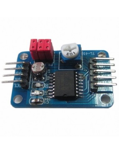
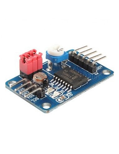


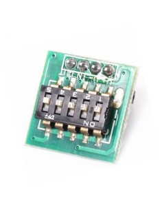
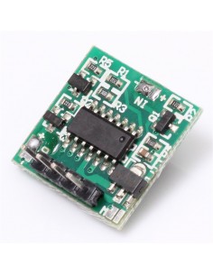
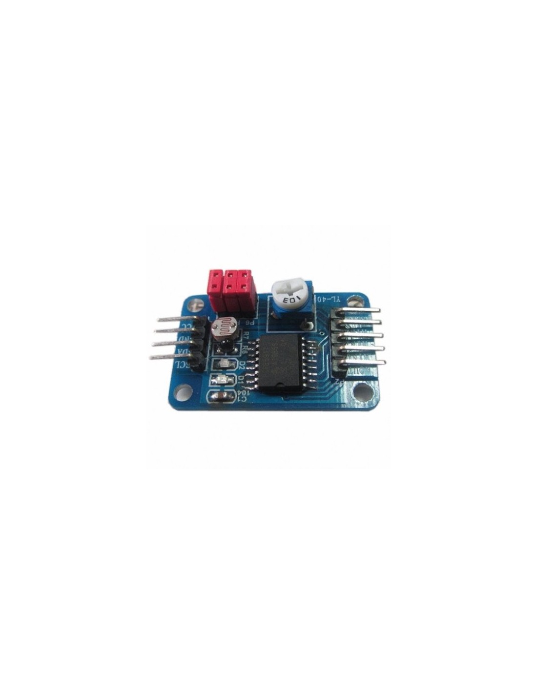
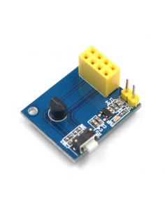
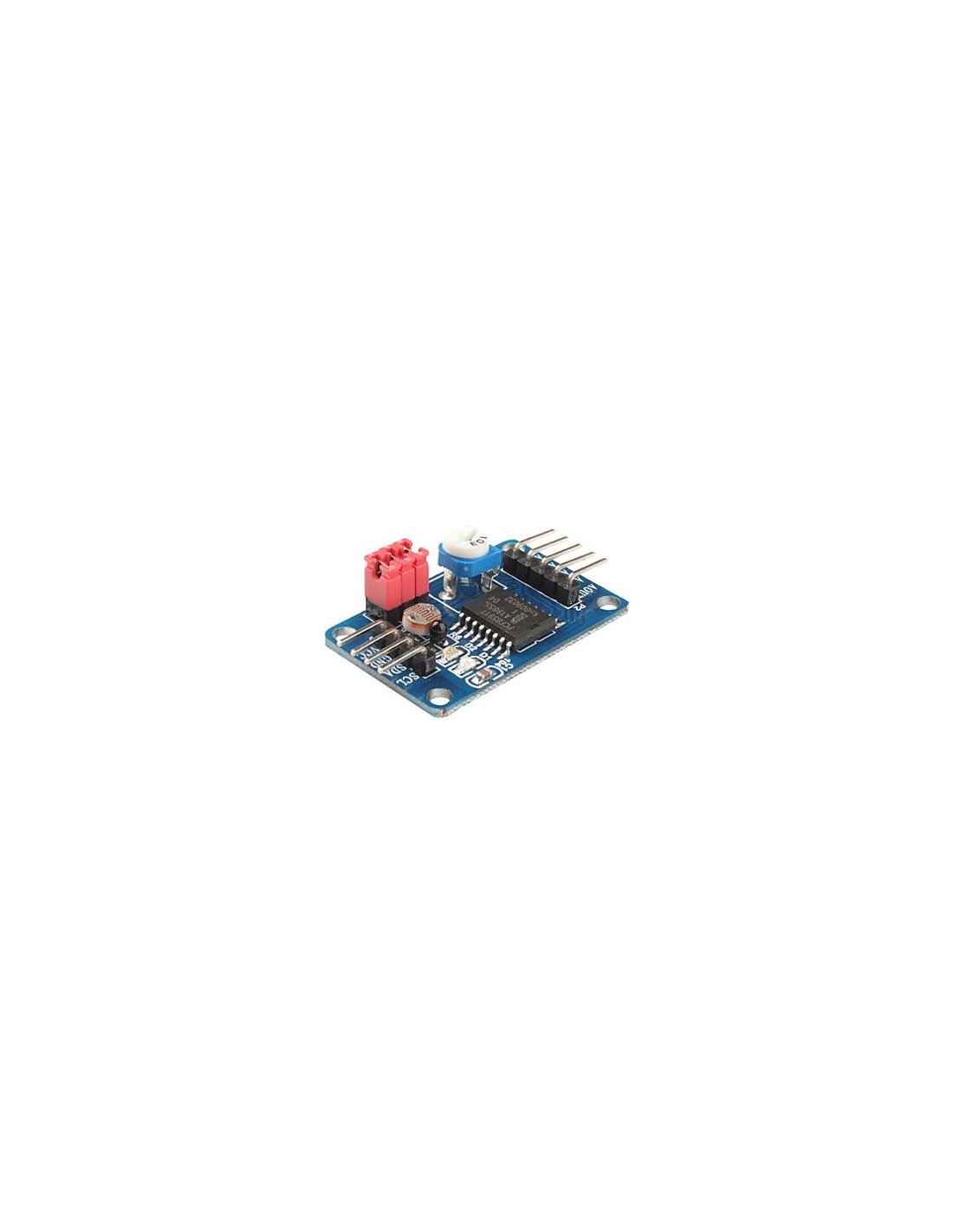
Converter ADC/DAC
The baby description:
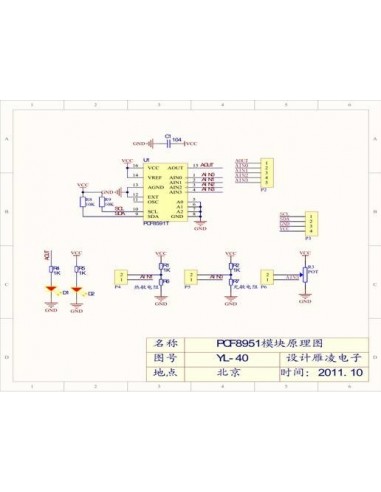
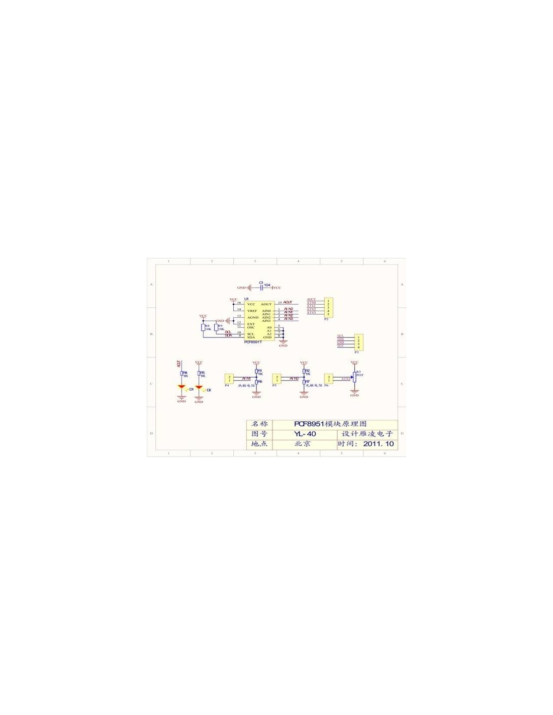
1. A module chip using PCF8951
2. module supports external voltage input capture (input voltage range 0-5v)
3. Three modules integrated photoresistor acquisition environment through the AD intensity accurate numerical
4. modules integrated thermistor, can capture the precise value of the ambient temperature through the AD
5. The five-module integrated 1 channel 0-5V voltage input acquisition (blue potentiometer to adjust the input voltage)
6. modules with power indicator light (on the module after power indicator lights)
7. modules with the DA output indicator light board DA output indicator module DA output interface voltage reaches a certain value, the voltage the greater the light brightness is more obvious;
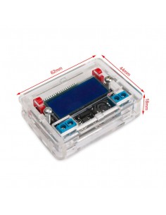
8. module PCB size: 3.6cm * 2.3cm
9. standard double-sided, plate thickness 1.6mm, the layout is nice, surrounded by the through-hole, aperture: 3mm, convenient fixed
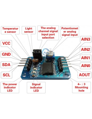
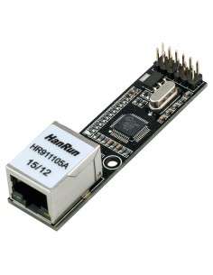
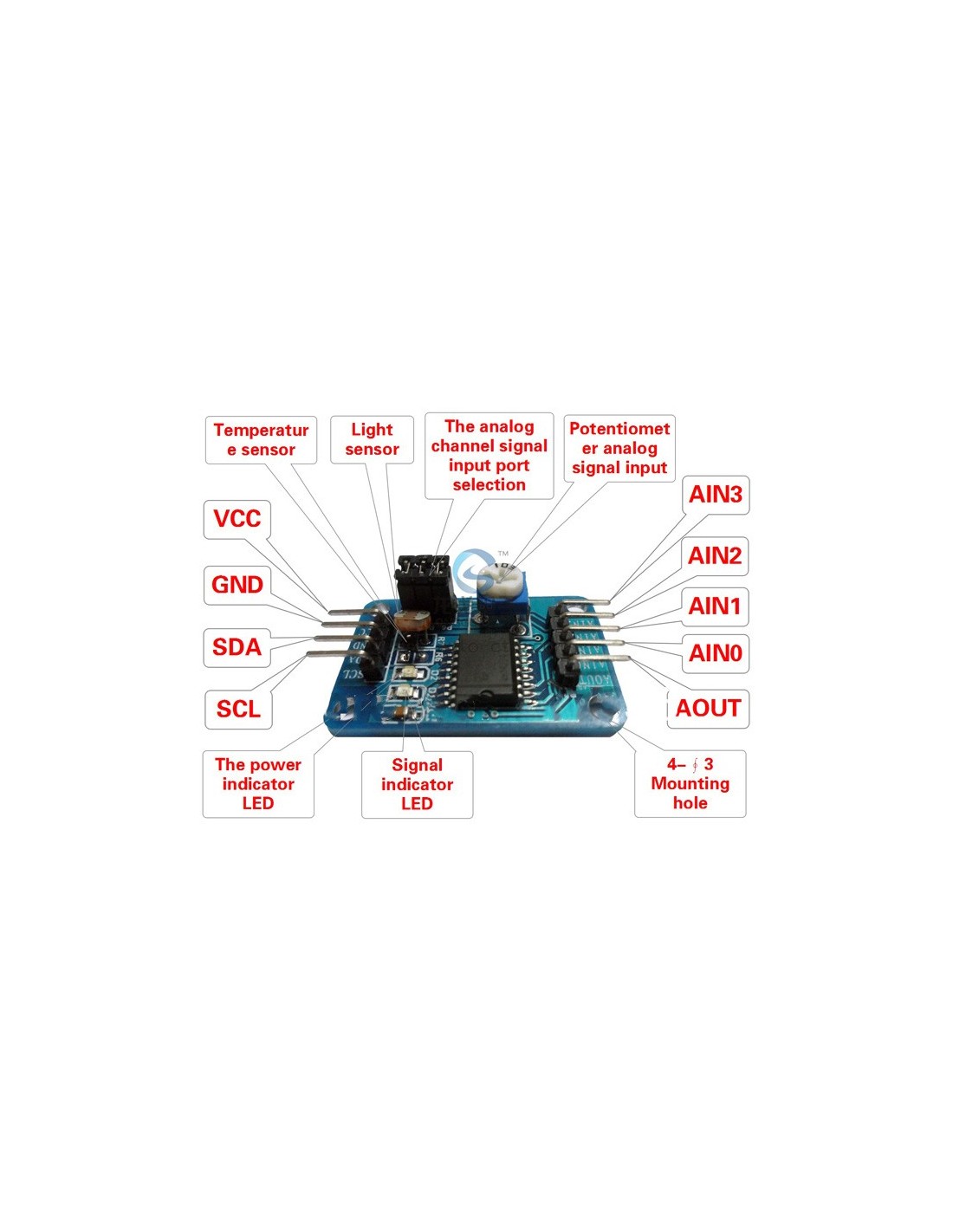
The module interface:
The module's left and right, respectively, the external expansion of 2-way pin interface, respectively, as follows:
Output interface of the left the AOUT chip DA
The AINO chip analog input interface.
AIN1 chip analog input interface
AIN2 chip analog input interface
AIN3 chip analog input interface
The right side of the SCL IIC clock interface to access the microcontroller IO port
The SDA IIC digital interface connected microcontroller IO port
GND module to an external
VCC power supply interface external 3.3v-5v
Module red jumper instructions for use
Module three red short circuit cap, respectively, the role are as follows:
P4 connected to the P4 jumper, select thermistor access circuit
P5 connected to P5 jumper to select the photoresistor access circuit
P6 connected to the P6 jumper, to select 0-5V adjustable voltage access circuit


